Search This Blog

Sunday, March 18, 2012

Programmable Logic Array (PLA)

Programmable Logic Array (PLA)


A programmable logic array (PLA) is a large Scale Integrated programmable logic device which is used for synthesizing combinational logic functions.  It consists of a programmable AND gate array followed by a programmable OR gate array. To synthesize the output logic functions, first of all these are needed to be reduced to their minimum sum of product expressions. In PLA implementation, a designer should try to deduce these expressions in such a way that maximum number of common product terms exist between them. All these product terms are then generated in the AND gate array. From there, these product terms are fed in to the OR gate array where they are added according to the deduced logic expressions in order to get the output functions.


Programmable Logic Array (PLA)

Both ROM and PLA can be used to implement arbitrary functions in the sum-of-product (SOM, actually OR-of-AND) form.


Example: Implement the following function by ROM and PLA: 

\begin{displaymath}f(A,B,C)=\sum (0,2,4,5,7) \end{displaymath}


This function is implemented by ROM as the OR of five minterms: 

\begin{displaymath}f(A,B,C)=A'B'C'+A'BC'+AB'C'+AB'C+ABC \end{displaymath}


ROM_PLA_a.gif
But after simplification by Karnaugh map:
pla_example_karnaugh.gif
the function can be implemented by a PLA as the OR of three terms:

\begin{displaymath}f(A,B,C)=AC+A'C'+AB' \end{displaymath}


ROM_PLA_b.gif
Note that in a PLA, only those terms that are needed are generated by the AND array, while in a ROM, all minterms have to be generated by the AND array.
pla_example.gif
pla_model.gif
MIPS_FSM_decoder_small.gif

Programmable Array Logic (PAL)


Programmable array logic (PAL)  

Programmable array logic (PAL) is a large scale integrated programmable logic device that is used for the synthesis of combinational as well as sequential logic. A PAL consists of a programmable AND gate array followed by a fixed OR gate array. This means that the PAL can be programmed to generate the required product terms in the AND gate array but the outputs of the AND gate array are connected in a fixed manner to the different OR gates of the OR gate array. Thus there is no need to find any common product terms between the different output logic functions and all the output functions are synthesized in their
minimum sum of product forms. 

Programmable Array Logic (PAL) Devices


The final programmable logic device to be discussed is the Programmable Array Logic or PAL device. The general structure of this device is similar to PLA, but in a PAL device only AND gates are programmable. The OR array in this device is fixed by the manufacturer. This makes PAL devices easier to program and less expensive than PLA. On the other hand, since the OR array is fixed, it is less flexible than a PLA device.


 represents the general structure of a PAL device. It has n input lines which are fed to buffers/inverters. Buffers/inverters are connected to inputs of AND gates through programmable links. Outputs of AND gates are then fed to the OR array with fixed connections. It should be noted that, all the outputs of an AND array are not connected to an OR array. In contrast to that, only some of the AND outputs are connected to an OR array which is at the manufacturer's discretion. This can be clarified by Figure 6.23, which illustrates the internal connection of a four-input, eight AND-gates and three-output PAL device before programming. Note that while every buffer/inverter is connected to AND gates through links, F1-related OR gates are connected to only three AND outputs, F2 with three AND gates, and F3 with two AND gates. So this particular device can generate only eight product terms, out of which two of the three OR gates may have three product terms each and the rest of the OR gates will have only two product terms. Therefore, while designing with PAL, particular attention is to be given to the fixed OR array. 

Tuesday, March 13, 2012

Basic Logic Gates & Boolean Expressions


Boolean Algebra
• Digital electronic systems manipulate binary information
• To design such systems we need a convenient
mathematical framework
– useful systems are often too complicated to keep in our head
– Boolean algebra provides this framework
• Points in a circuit are represented by Boolean Variables
• Boolean algebra allows us to specify relationships
between Boolean variables
– Hence Boolean algebra can be used as a design tool for digital
electronic circuits

Boolean Variables
Boolean variables take the value either 0 or 1 only
– if a variable doesn't have the value 0, then it must have the value 1
– if a variable doesn't have the value 1, then it must have the value 0
• In digital electronics:
– Boolean 0 and 1 correspond to the binary 0 and 1
• In logic:
– 1 and 0 are sometimes called true and false
• We use symbols to represent Boolean variables
– just like with ordinary algebra
– eg: A, B, C, X, Y, Z, etc
– typically a single character
– typically upper case
• Three Logic operations: AND, OR, NOT

 Boolean Algebra to Describe Logic
• Boolean representation: 4 variables H, R, F and S
• H represents the On/Off switch of the entire heating
system
– H = 1 when the heating system is switched on.
• R represents the room thermostat
– R = 1 when the room temperature is lower than required
• F represents the frost thermostat
– F = 1 when the external temperature is near freezing
• S represents the On/Off switch of the boiler
– S = 1 when heat should be generated by the boiler 
• S should be 1 when (H=1 and R=1) or when (F=1 and
R=1)
• In Boolean algebra we use  for 'and' and + for 'or'
S = H • R + F • R
• If we could build an electronic circuit which implemented
this Boolean expression we could sell it as a simple
heating system controller.
Boolean Operators 
– Like ordinary algebra, Boolean algebra allows for 
operations on its variables
• NOT - Takes the complement (inverse) of a single variable
– Called 'NOT K' and written K
• eg: Let K represent a key on a computer keyboard and let K = 1 
mean the key is pressed
– We now have a variable which shows the state of the key:
• K=1 shows key is pressed
• K=0 shows key is not pressed
– If we take the compliment of K we have a variable which 
also shows the state of the key but in the opposite sense
• K=1 shows key is not pressed
• K=0 shows is pressed
Basic Boolean Operators & Logic Gates 


Summary of OR operation

• Produce a result of 1 whenever any input is 1. 
Otherwise 0.
• An OR gate is a logic circuit that performs an OR 
operation on the circuit's input
• The expression x=A+B is read as “x equals A 
OR B”


Summary of the AND operation

• The AND operation is performed the same as 
ordinary multiplication of 1s and 0s.
• An AND gate is a logic circuit that performs 
the AND operation on the circuit’s inputs.
• An AND gate output will be 1 only for the 
case when all inputs are 1; for all other cases 
the output will be 0.
• The expression x=A•B is read as “x equals A 
AND B.”


Sunday, March 11, 2012

555 timer


EXPERIMENT

PROBLEM STATEMENT:
We create a 555 timer circuit that you can control the light produce by the LED.

Equipment we used:
555 timer
Potentiometer
1k ohm resistor
10k ohm resistor
20k ohm resistor
20 microfarad capacitor
LED
Breadboard
20k ohm potentiometer


ASSEMBLY INSTRUCTIONS:
555 timer
In setting our 555 timer, the first thing to do is to determine what will be our time and period. Before assembling it on the breadboard, we familiarize the pin configuration of the 555 timer and the resistors. Since we are already familiar of the pin configuration of the following materials, we assemble these materials in the breadboard. 

 SCHEMATIC DIAGRAM
As we conduct the experiment, as we increase the value of the potentiometer,
the light of the LED will increase depending on the value of the potentiometer.
The Higher the value of the potentiometer, the more light will produce by the LED.
And in this plate, we get to familiarize the use of the 555 timer which we will be used in the future plates in this subject and we will enjoying this because we learned a lot. 


OUTPUT


Saturday, March 10, 2012

Logic Circuit

We have a problem that we need to solve. 
This is all about the topic of DON'T CARE TERM.


PROBLEM STATEMENT:

A Seven-SegmentDisplay (SSD), or Seven-Segment Indicator, is a form of
electronic display device for displaying decimal numerals. Seven-segment displays
are widely used in digital clocks, electronic meters, and other electronic devices for
displaying numerical information (en.wikipedia.org/wiki/Seven-segment_display).


In this activity, the students should be able to display decimal numerals using binary
coded decimals via the SSD.

A discussion of the types of SSD and its corresponding pin configurations should be
included in the text.


after that we identify the materials that we will used such as:

3 PCS LM7400 :


1 PC LM7410:
2 PCS LM7420:
1 PC LM7404:
1 PC LM7432:


7 segment display


ASSEMBLY INSTRUCTION:

This Project is a BCD to Decimal numbers converter, which displays the inputted BCD number in the seen segment display as a decimal number.
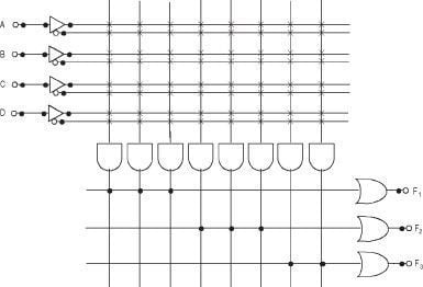
Firstly, the BCD (binary coded decimal) is a code format in which decimal digits (0-9) are expressed as four digit binary numbers. And here we are inputting those BCD values using 4 inputs which are connected to the DIP switch, those 4 inputs are for the 8 bit binary numbers which are (1, 2, 4 and 8), and  whichever the input is will be displayed in the seven common cathode display. A seven display, as its name indicates, is composed of seven elements. Individually on or off, they can be combined to produced simplified representations of the decimal numbers. Each element of the seven-segment display is a small light emitting diode(led) or liquid crystal display(LCD), those are assigned as letters A to G.
We had used a 330 ohm resistor for each of the outputs for the seven segment display, for the safety purpose and to avoid heat on the seven segment display because of much bigger current sent from the source. By using these resistors which are in series on each segment of the display, we reduced the current entering to the segment.


FOR SCHEMATIC DIAGRAM:


TRUTH TABLE:

W
X
Y
Z

a
b
c
d
e
f
g
0
0
0
0

1
1
1
1
1
1
0
0
0
0
1

0
1
1
0
0
0
0
0
0
1
0

1
1
0
1
1
0
1
0
0
1
1

1
1
1
1
0
0
1
0
1
0
0

0
1
1
0
0
1
1
0
1
0
1

1
0
1
1
0
1
1
0
1
1
0

1
0
1
1
1
1
1
0
1
1
1

1
1
1
0
0
0
0
1
0
0
0

1
1
1
1
1
1
1
1
0
0
1

1
1
1
1
0
1
1
*
*
*
*

*
*
*
*
*
*
*
*
*
*
*

*
*
*
*
*
*
*
*
*
*
*

*
*
*
*
*
*
*
*
*
*
*

*
*
*
*
*
*
*
*
*
*
*

*
*
*
*
*
*
*
*
*
*
*

*
*
*
*
*
*
*
*
*
*
*

*
*
*
*
*
*
*


This plate is a process of making a circuit converting a binary input to a decimal output using a seven segment display. Using a 4-bit truth table we come up with an equation in every segment converted in a schematic diagram. This plate is for a student to learned and to enjoy.

 We're enjoying constructing this kind of plate after that we finish this plate and we feel so great because we finish and our work is working..